Dicing takes place near the end of the semiconductor process flow. At this point the silicon wafer is finally turned into individual chips, or die, traditionally by means of a saw or laser. (Check out the first article in our Plasma Dicing 101 series, which compares traditional dicing methods such as blade and laser to plasma dicing).
“Plasma dicing has gained acceptance within the semiconductor industry as a viable solution versus blades or lasers, particularly as chips get smaller, thinner and more complex.”
Richard Barnett, director, Etch Product Management


Plasma Dicing: An in-Depth View
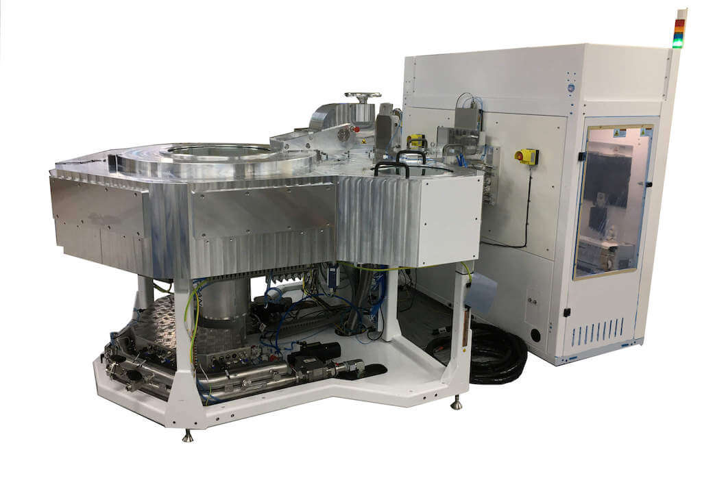
Plasma dicing uses the Bosch silicon etch process, a multistep method that alternates between deposition and etching to create features in the wafer. The chemical reaction between the silicon and fluorinated chemistry is exothermic, meaning that heat will be generated by the process itself. The Rapier-S process module is designed to manage this through the use of electrostatic clamping. Keeping the wafer in close contact with the cooled platen allows the process to run, preserving the die and tape without any risk of damage being caused by overheating.
Cleaner Processing
Plasma dicing is an extremely clean method of singulation. Unlike blade or laser dicing, no particles are produced by the plasma method. During the dicing etch process, the silicon reacts with the fluorine and is simply vaporized. Fluorocarbon polymers, which are a key element of the Bosch process, can remain on the side walls of the etched feature after the etch has been completed. There are, however, subsequent steps to remove these completely, making plasma dicing the cleanest method compared to blade or laser. This cleanliness is crucial for the integration steps where die are bonded to others, creating a complex multi-die package. Successful bonding requires clean surfaces and die edges to prevent any voids in the bonding interface.
More Die per Wafer
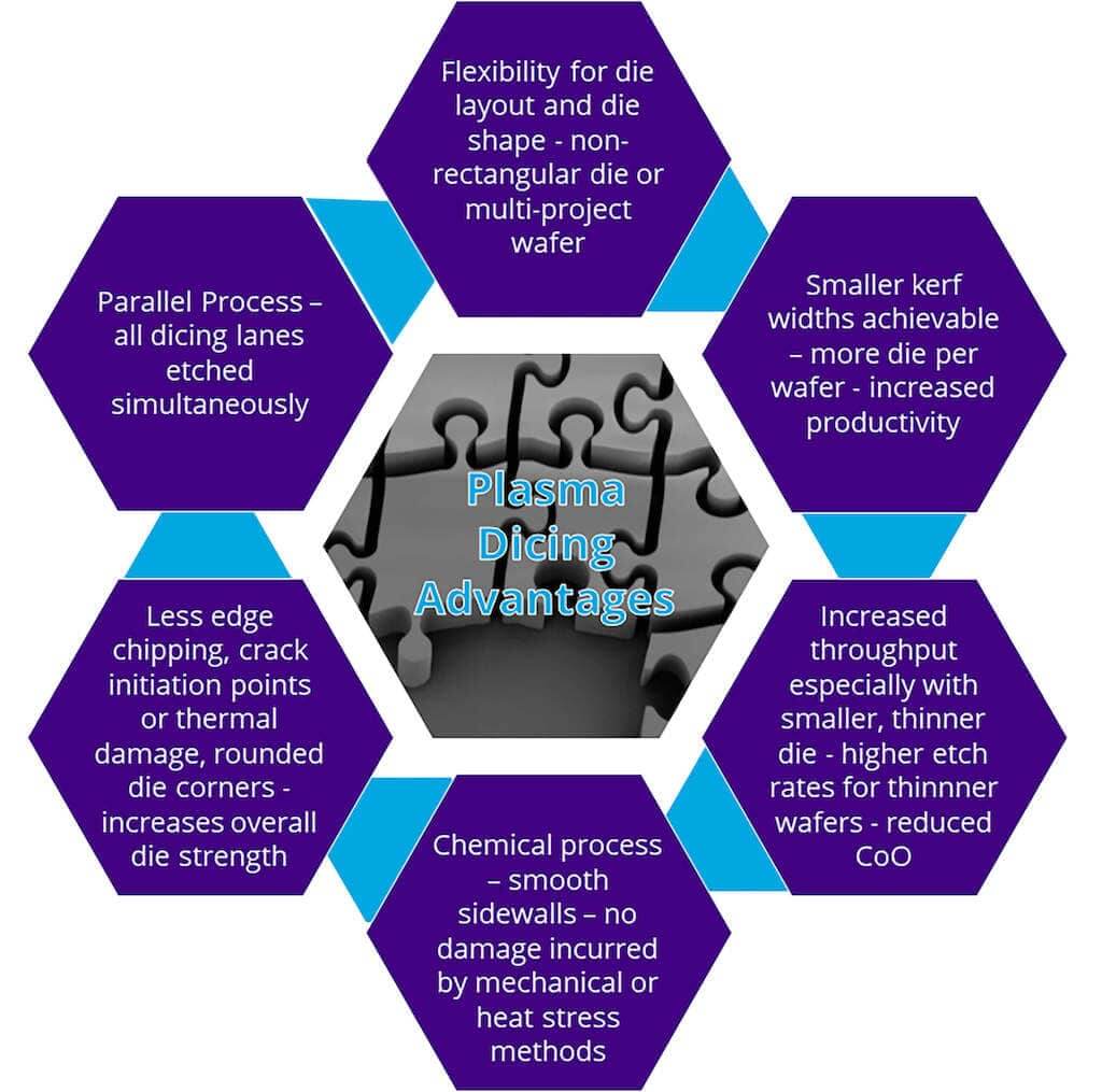
With plasma dicing, chip manufacturers can use much narrower kerf widths (dicing lanes or the space between die reserved for cutting the wafer). This is particularly useful when dealing with small die such as RF-ID tags (typically <0.5mm x 0.5mm). By moving to plasma dicing, valuable wafer real estate is no longer wasted but becomes available for adding more product onto each wafer. This gain can be huge, depending on the die sizes, and reduce the overall need for additional wafers, process materials and front-end equipment to increase output.
Stronger Die
The ability to maintain die integrity after dicing is equally as important. Plasma dicing is the preferred method to preserve die strength because alternative dicing methods are known to cause damage such as internal and surface cracks, heat-affected zones or chipping.
In a paper published by imec it was found that the die strength after plasma dicing was higher than all other dicing methods tested, which included laser groove (with and without plasma dicing) and laser groove with stealth and blade dicing. Furthermore, die singulated by plasma have the best bonding performance as no voids were found around the die periphery. imec concluded that for die-to-wafer bonding, plasma dicing was the better solution for die singulation prior to the bonding stage.
Hybrid Bonding … and Why Die Integrity Matters
Hybrid bonding is the process to create a permanent bond between heterogeneous die using tiny copper pad connections as opposed to traditional microbumps. This method of connecting die can increase interconnect density and functionality in advanced 3D device stacking – delivering up to 1,000 times more input-output connections than copper microbumps and driving signal delay to near-zero levels. Hybrid bonding improves performance without any power and signal penalties. Further advantages include expanded bandwidth, higher memory density and increased power and speed efficiencies.
With an increased density of smaller interconnects, surface cleanliness becomes critical to enable reliable die-to-wafer hybrid bonding and optimize yields. Any particulate debris or laser damage to the surface may prevent die surfaces from contacting the wafer correctly and result in incomplete bonding. Die integrity is also important to withstand the stresses and strains of being bonded and stacked. If there was a failure in any single die, that would cause a failure in the entire chip stack.
Production Proven
High volume manufacturing has many requirements for successful implementation of process steps. Automated end-point detection (EPD) is essential for many wafer etch applications to make sure processes are carefully controlled and consistent, resulting in high yields, wafer-after-wafer. The wafer is diced while mounted on a tape surface in a film frame carrier to keep the die held in place once the dicing is complete. Protecting the tape as the plasma dicing process approaches its endpoint is critical to complete die singulation without exposing the tape to excessive heat or plasma attack. KLA Claritas and Sentinel process monitoring and control systems offer the necessary oversight of the process and substrate conditions to achieve this.
Depending on the die size, the throughput of plasma dicing can surpass all other methods, as it is a single-pass method where the wafer is processed only once; blade and laser tools can require multiple passes across the wafer, adding to the overall step time. Additionally, when the need for expansion arises, KLA cluster platforms save essential floor space within the wafer fab by adding process chambers onto the existing handler.

Packaging manufacturers continue to optimize their operations with full automation to move wafers around the factory by overhead track (OHT) or auto-guided vehicles (AGV). KLA supports these enhanced wafer handling capabilities for plasma dicing. The Mosaic OHT is designed for up to four process modules and can run a mix of film frame carriers (FFC) and wafers in parallel with the automated overhead transport.
Semiconductor Innovation Demands High Quality
Plasma dicing is a proven alternative to conventional singulation methods of using saw blades or lasers and is required for innovative new technologies within the industry.
Summary of key benefits:
- High silicon etch rates for high wafer/die throughput
- Cleaner method of singulation, crucial for any subsequent integration steps when die are bonded to others to create a complex multi-die package
- Small kerf widths release valuable wafer real estate, which can be used for more active die per wafer, eliminating the cost of additional wafers and front-end equipment
- Preserves die strength by eliminating damage associated with laser or saw dicing
- Automated end-point detection (EPD) to ensure processes are carefully controlled and consistent for high yields in production
- Choice of wafer and frame handling platforms designed to take plasma dicing from R&D and prototyping to high volume production
To learn more about the advantages of plasma dicing over traditional methods and how they impact manufacturing processes, send us an email.
Follow Us