Introduction
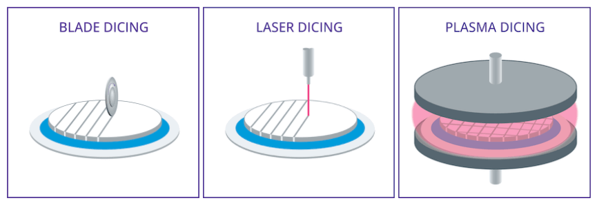
Taking place at the end of the semiconductor process flow, dicing is the process where the silicon wafer is finally turned into individual chips, or die, traditionally by means of a saw or laser. A saw blade, or laser, is used to cut the wafer along the areas between the chips called dicing lanes. This step separates the chips from the wafer making them ready to be packaged and fitted to whichever device they will end up in.
Plasma dicing achieves the same outcome with a dry etching process that uses a fluorine plasma to etch away the material in the dicing lanes between the chips. Plasma dicing is gaining acceptance within the semiconductor industry as the preferred solution, versus blades or lasers, particularly as chips get smaller, thinner and more complex.

What is blade dicing?
Blade dicing is the process of using an abrasive disc (blade) rotating at high speed to cut along the dicing lanes. Typically, the blade tip is made of abrasive grit or extremely thin diamond, and can be used to dice through, i.e., cut, or simply groove the silicon wafer. However, just like any mechanical cutting method, blade dicing relies on physical removal of material that can cause chipping and cracking of the die, resulting in damaged product and lower yields.
What is laser dicing?
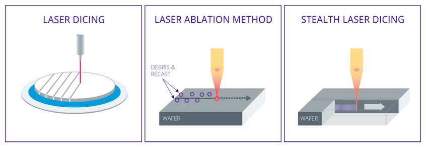
Laser dicing, as the name suggests, uses laser technology to separate the wafer into die. The process involves delivering high concentrations of photon streams onto the wafer, generating a spot of high localized temperature to remove the dicing lane area, between the chips. The laser heats the material to such a temperature, that the area under the laser spot is blown away (ablated) or simply vaporized. The laser can also be focused to deliver this heat into the bulk of the wafer, this method is called “stealth” laser dicing. For this approach, the heat from the laser creates voids within the dicing lane. These weakened regions then act like a perforation and tear apart when the wafer is expanded. In comparison to the blade saw method, laser dicing is considerably more costly.

Why choose plasma dicing?
Plasma dicing offers many benefits in comparison to other traditional dicing methods.
Increased yields
Plasma dicing removes the material in the dicing lane chemically. There is no mechanical damage, no heat affected zones or other physical impact on the die. This means that plasma dicing causes no damage. Die, singulated by plasma, have higher break strength compared to those singulated by blade or laser.
This gain in mechanical integrity is a particular advantage for die subject to physical stresses in service, such as those used in hybrid bonding stacks for high bandwidth memory (HBM), where if one chip in the stack fails, the whole device is lost.
With a move toward much thinner die, the non-mechanical nature of plasma dicing is a valuable attribute as industry roadmaps push thicknesses below 50µm.
Increased throughput
Blade dicing and laser dicing are “serial” processes cutting along the dicing lanes one after the another. For laser, specifically, multiple passes may be needed. Plasma dicing removes all the dicing lanes “in parallel” at the same time. This means as die sizes shrink (i.e., more dicing lanes and therefore more cuts required), and wafers get thinner (less silicon for plasma to remove, or lower blade speeds/ laser powers needed to avoid damage), there are cross-over points where plasma dicing becomes the fastest process.
Increase in die per wafer
Without any physical restrictions such as blade width, or laser spot size, to accommodate plasma can enable a move to narrower dicing lanes, providing an opportunity to increase the die output of a production line. Freeing up wafer real-estate, previously sacrificed for the mechanical singulation method, can now be allocated to additional active die. The potential for die count gains is significant, particularly when smaller die sizes are considered.
Design flexibility
As the wafer layout is not constrained by the need to have linear dicing paths, plasma dicing can offer device designers much greater flexibility with regard to fundamental die shape/size, removing guard rings and positioning of die/test groups to make better use of the wafer area.

Attractive for fragile devices
Plasma dicing is also attractive for fragile devices such as micro-electro-mechanical systems (MEMS). For example, inertial sensors which consist of tiny movable structures would stand to benefit from a clean, non-mechanical singulation method. There would be no physical forces to vibrate the wafer and cause damage to the sensing features, or particles to jam in between them and affect their movement.
Eliminate particulate contamination
The chemical nature of plasma dicing produces only gaseous by-products which are removed by vacuum pumping leaving a clean wafer surface, critical in applications such as hybrid bonding. Mechanical dicing or laser ablation can result in debris or particulate contamination across the wafer surface (which can be detected using the ICOS™ F160XP die sorting and inspection system) even with careful cleaning/drying.
Summary
So, while conventional dicing methods will continue to be a cost-effective solution for many applications, there are a growing number of cases where plasma dicing can offer greater yields, flexibility and throughput, resulting in a lower cost of ownership overall. Learn more about the benefits of plasma dicing in our Tech Insights articles or by watching our recent SPTS Webinar.
If you would like to discuss your own dicing requirements and find out if SPTS plasma dicing can solve any issues with your current solution, get in touch with us.
Check out the Chip Manufacturing 101 post to learn more of the basics of semiconductor manufacturing and the key role KLA’s process control and process enabling solutions play in the manufacturing supply chain.
If you’re interested in being part of the next technological breakthrough and advancing humanity with us, browse our careers page.
Follow Us