- MEMS
- Advanced Packaging
- RF Device Manufacturing
- Power Device Manufacturing
- Photonics
Etch
Etching is a term used in chip manufacturing to describe any process which removes material from the wafer surface. By using a mask to protect selected areas of the wafer surface it is possible to etch features to create the desired microstructure for the device. KLA offers a number of dry etch technologies which either expose the wafer surface to reactive ions in a plasma (formed by RF excitation of a low pressure process gas), or a gaseous etchant such as HF or XeF2 vapor.
Product Categories
SPTS Omega® with Rapier™/DSi-v Module
Plasma Etch Systems for Silicon
The SPTS Omega® Rapier™ and DSi-v process modules offer high rate silicon etching for a variety of applications. Deep reactive ion etching (DRIE) of silicon uses the Bosch Process, which switches the plasma chemistry repeatedly between etch (SF6) and passivation(C4F8) steps, to create anisotropic etching of trenches or holes into silicon. With an installed base of >1500 DRIE process modules, KLA has decades of expertise in deep silicon etching for MEMS and other applications. The SPTS Rapier™ offers a dual plasma source design with independently controlled primary and secondary decoupled plasma zones, with independent dual gas inlets. This results in a highly concentrated and uniform distribution of radicals, resulting in high etch rates, excellent cross-wafer uniformity and control of CD, profile and feature tilt. This performance can be realized on wafers up to 300mm diameter. Inherent multi-mode flexibility also allows complementary oxide etching within the same hardware. The SPTS DSi-v module, offers excellent deep silicon etch performance for high load applications. The DSi-v is especially suited to large cavity etches for applications such as silicon microphones or pressure sensors. The Rapier™ and DSi-v are both compatible with the Omega® LPX, c2L or fxP wafer handling platforms, or integrated with different SPTS etch and deposition modules on a Versalis™ cluster platform.
Market Brochures
Patented dual plasma source design with independently controlled primary and secondary decoupled plasma zones, with independent dual gas inlets. This results in a highly concentrated and uniformed distribution of radicals.
- High etch rate
- Excellent uniformity
- Controls tilting of deep features across the wafer
Inherent multi-mode flexibility also allows complementary oxide etching within the same hardware.
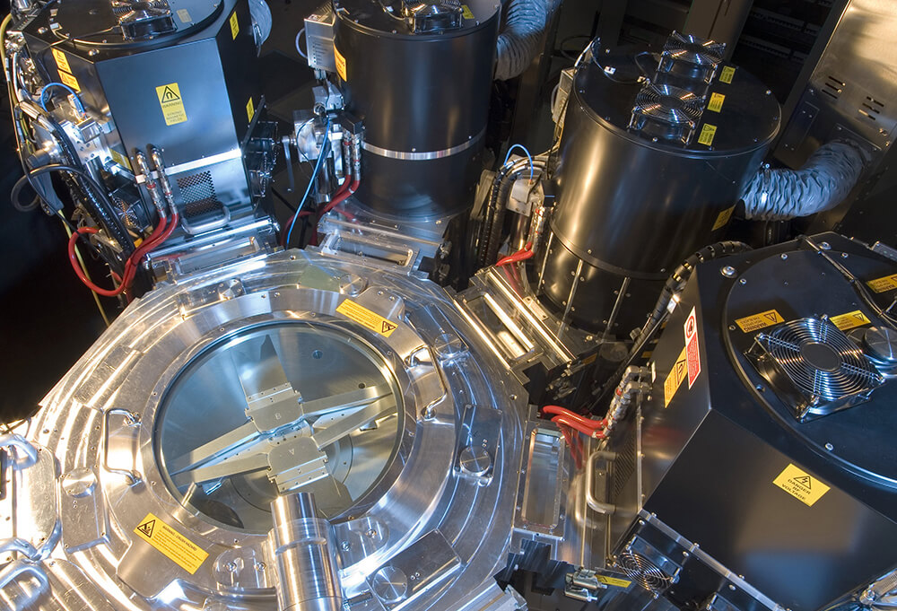
SPTS Omega® fxP with Rapier and DSi-v modules
- Deep reactive ion etch (DRIE) of Si for MEMS micromachining, TSVs, power trenches, backside Si vias
- Blanket Si etching for via reveal and wafer thinning
- Shallow oxide etch
SPTS Omega® with SynapsEtch Module
Plasma Etch Systems for Strongly Bonded Materials
The SPTS Omega® SynapsEtch process module uses a high density plasma source to etch strongly bonded materials. The SPTS Omega SynapsEtch etch process module is heated and has a magnetic confinement chamber giving a higher plasma density than conventional ICPs (by a factor of ~10x). This higher plasma density means higher etch rates can be achieved for strongly bonded materials. The Omega SynapsEtch is routinely used for etching of deep features in dielectric materials including silicon oxide, quartz and glass. Other low volatility materials, such as SiC, AlScN, are also easily processed by the Omega SynapsEtch module. The Omega SynapsEtch is compatible with the LPX, c2L or fxP wafer handling platforms, or integrated with different SPTS etch and deposition modules on a Versalis™ cluster platform.
- MEMS
- RF Device Manufacturing
- Power Device Manufacturing
- Photonics
Market Brochures
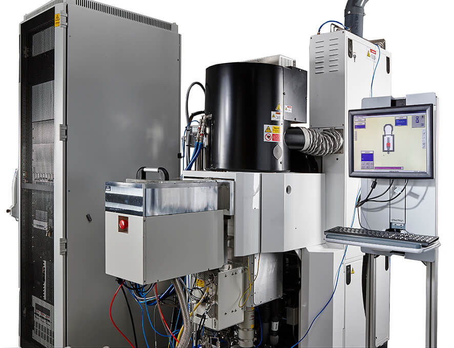
SPTS Omega® LPX SynapsEtch
- Unique source design creates high ion density for increased etch rate of strongly bonded materials
- Heated process chamber for improved mean time before clean (MTBC)
- Deep high rate oxide etching
- Glass etch
- High rate SiC etch
- SiN etch
- GaN etch
- PZT and AlScN etch
- Al2O3 etch
SPTS Omega® with ICP Module
Plasma Etch Systems for a Wide Range of Materials
The SPTS Omega® ICP process module is highly flexible and etches a wide range of materials including GaAs, GaN, SiN, oxides, polymers, low aspect ratio Si and metals. The SPTS ICP process module uses a high density plasma source incorporating a radial coil design. Used in applications for RF devices and photonics/optoelectronics devices, the ICP process module is an enabling tool for the semiconductor industry. The ICP module is compatible with the Omega® LPX, c2L or fxP wafer handling platforms, or integrated with different SPTS etch and deposition modules on a Versalis™ cluster platform.
- RF Device Manufacturing
- Photonics
Market Brochures
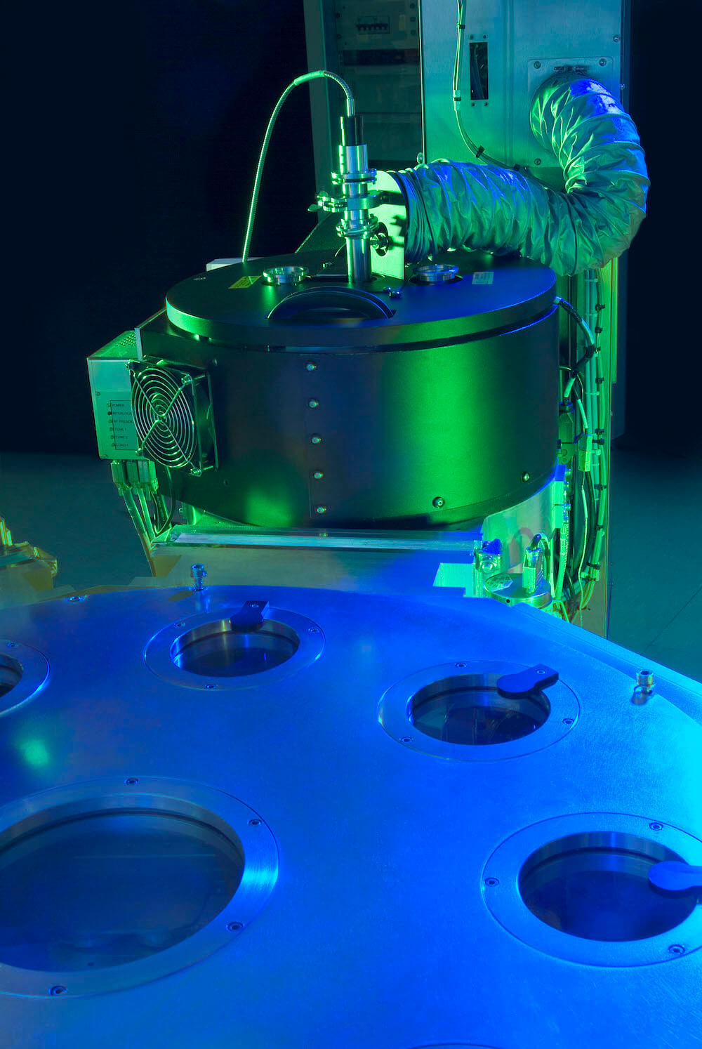
Omega® fxP ICP
- Flexible processing for a wide range of etch applications and materials
- Low damage etch processes
- GaAs etch
- GaN etch
- SixNy etch
- BCB and Polyimide etch
- Metal etch
- Low aspect ratio Si etch
SPTS Mosaic™ with Rapier-S/Rapier-300S Module
Plasma Dicing Systems
Plasma dicing, using Deep Reactive Ion Etching (DRIE) processing, is a viable alternative to conventional singulation methods using saw blades or lasers. Plasma dicing offers considerable benefits to users, including narrower kerf widths that allow >80% more die per wafer (depending on die size). Cleaner processing improves yields in die-to-wafer hybrid bonding. Based on a chemical removal of material, plasma singulation increases die strength and improves die reliability in critical applications.
The SPTS Mosaic™ plasma dicing systems offer plasma singulation of die from a silicon wafer (up to 300mm, on frames). The Rapier-S module is based on the well-established "dual-source" Rapier module giving an extremely uniform and controllable plasma profile, and is capable of handling taped wafers on 296mm or 400mm frames. The SPTS Mosaic™ OHT cluster platform accommodates 4 process modules and is compatible with both 296/400mm frames and 200/300mm wafers (in parallel) and includes an industry-standard EFEM with 2/3 loadports which can receive overhead transport.
Advanced Packaging
Market Brochures
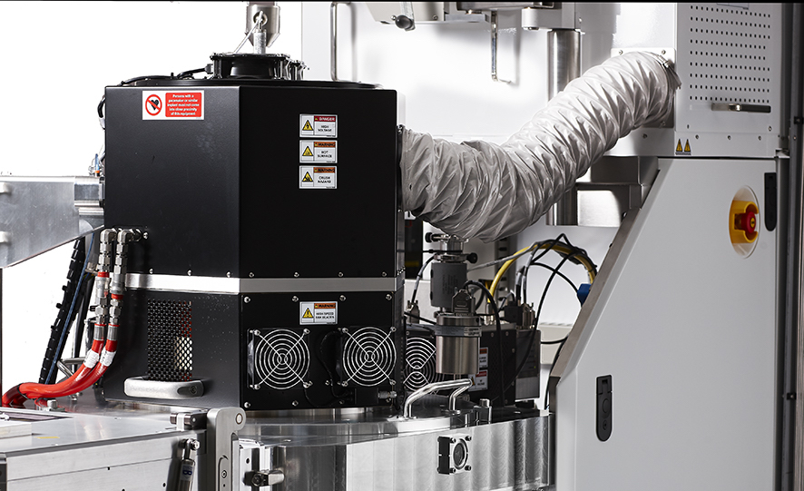
Rapier 300S module
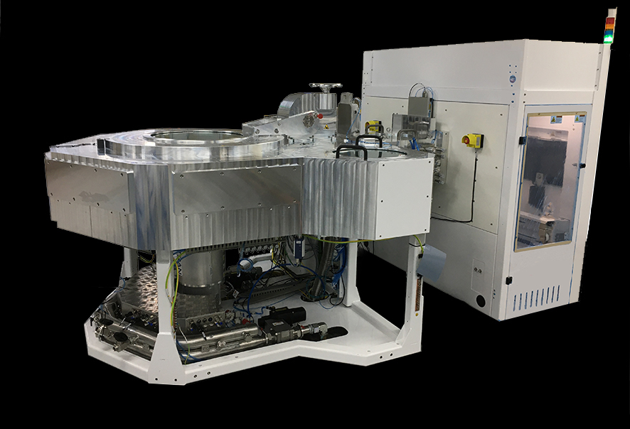
Mosaic OHT Platform
- High rate, low damage Si etch technology
- Choice of wafer handling options for wafers and/or frames
- Patented Claritas™ and Sentinel™ for endpoint / wafer protection
- Optional Defender™ defluorination module to remove residual fluorine, if required
Plasma dicing of silicon
Primaxx® Monarch 300
HF Vapor Etch System for 200/300mm Wafers in Volume Production
The Primaxx® Monarch 300 vapor hydrogen fluoride (VHF) etch system is fully integrated and designed to perform selective MEMS etch release via a controlled anhydrous HF/alcohol etch process. This system is compatible with 200mm and 300mm wafers, offering high throughput, high uptime batch processing for up to 13 wafers per batch. Extensive process control and monitoring functions ensure the yield, reliability and repeatability required in volume production.
The Monarch 300 is compatible with the Primaxx® 300 fxP wafer handling platform and supports up to 6 VHF etch process modules. This VHF etch module can also be combined with other SPTS etch or deposition modules on a SPTS Versalis™ platform, if required.
- MEMS
- RF Device Manufacturing
- Photonics
- Advanced Packaging
Market Brochures
- Compatible with 200 and 300mm wafers
- Batch size up to 13 wafers
- Available on Primaxx 300mm fxP platform (or Versalis fxP)
- Small footprint includes process chamber, gas/liquid panel and pressure/vacuum components
- MEMS release etch
- MicroLED release
- Vapor release of RF devices
Primaxx® Monarch 25
HF Vapor Etch System for Wafers up to 200mm in High Volume Production
The Primaxx® Monarch 25 vapor hydrogen fluoride (VHF) etch system is fully integrated and designed to perform selective etch release via a controlled anhydrous HF/alcohol etch process for medium to high volume HF release etch production applications. The Primaxx Monarch 25 is compatible with wafers from 100mm-200mm (4-8”), offering high throughput, high uptime batch processing for up to 25 wafers per batch. Extensive process control and monitoring functions ensure the yield, reliability and repeatability required in volume production. Process chamber, gas/liquid panel, and pressure/vacuum components, all within a small footprint. The Monarch 25 is available on either the Primaxx® fxP (for up to 6 process modules) or Primaxx® c2L (up to 4 process modules) platforms. This VHF etch module can also be combined with other SPTS etch or deposition modules on a SPTS Versalis™ platform if required.
- MEMS
- RF Device Manufacturing
- Photonics
Market Brochures
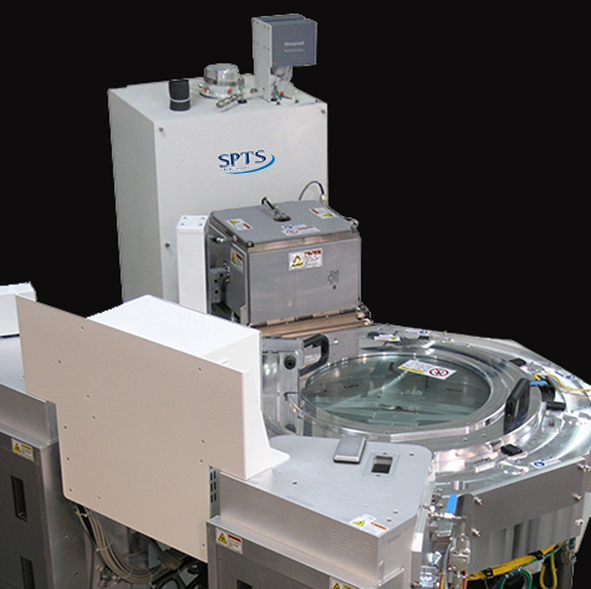
Primaxx® fxP Monarch 25
- Compatible with 100mm-200mm wafers
- Batch size up to 25 wafers
- Available on Primaxx c2L, Primaxx 200mm fxP and SPTS Versalis platforms
- Small footprint includes process chamber, gas/liquid panel and pressure/vacuum components
- MEMS release etch
- MicroLED release
- Vapor release of RF devices
Primaxx® Monarch 3
HF Vapor Etch System for R&D and Small Batch Processing
The Primaxx® Monarch 3 vapor hydrogen fluoride (VHF) etch system is designed to perform selective etch release via a controlled anhydrous HF/alcohol etch process. The Monarch 3 is a compact module includes a 3-wafer process chamber including a semi-automatic 3-wafer loader with load lock, and is designed for research laboratories and small volume production environments. An integrated panel PC, with on-board electronics minimizes cleanroom footprint and the system has been designed for easy wafer size changes and maintenance.
- MEMS
- RF Device Manufacturing
- Photonics
Market Brochures
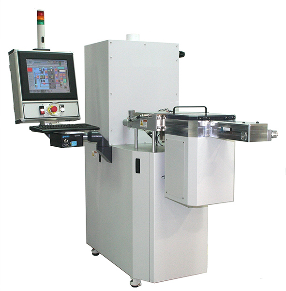
Primaxx Monarch 3
- Compatible with 100mm-200mm wafers
- Batch size up to 3 wafers
- Standalone system
- Small footprint includes process chamber, gas/liquid panel and pressure/vacuum components
- MEMS release etch
- MicroLED release
- Vapor release of RF devices
Primaxx® uEtch
HF Vapor Etch Systems for Single-Wafer Processing in R&D Applications
The Primaxx® uEtch compact single-wafer HF vapor etch system is specifically designed for university and small research laboratories. The fully integrated system includes a built-in HF gas cabinet, which can process single whole wafers (100-200mm) or die on a carrier. PLC (Programmable Logic Controller) control gives multi-user features and extensive safety interlocks. HF vapor processes developed on the uEtch are transferable to Primaxx Monarch 3, Monarch 25 and Monarch 300 production systems, offering a path from concept to production.
- MEMS
- RF Device Manufacturing
- Photonics
Market Brochures
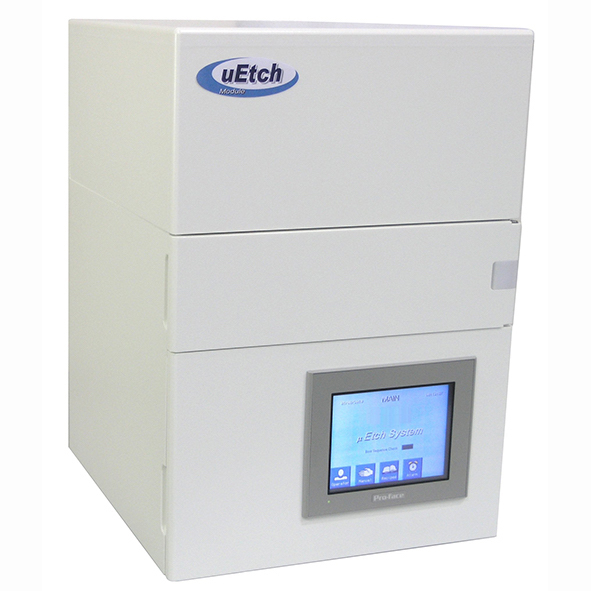
Primaxx uEtch
- Fully integrated, compact system includes built-in HF gas cabinet
- PLC controlled with multi-user features and extensive safety interlocks
- Can process single whole wafers (100-200mm) or die on a carrier
HF vapor processes are transferable to SPTS 3- and 25-wafer production systems, offering a path from concept to production
- MEMS release etch
- MicroLED release
- Vapor release of RF devices
Xactix® CVE
XeF2 Vapor Etch Release System for High Volume Production
The Xactix® CVE xenon difluoride (XeF2) etch module has a unique chamber design which provides high etch rates, uniformity and efficiency. Isotropic etching of silicon using XeF2 is an ideal solution for releasing MEMS or photonic devices. XeF2 shows high selectivity to silicon over almost all standard semiconductor materials including photoresist, silicon dioxide, silicon nitride and aluminum. The Xactix CVE module is compatible with the c2L or fxP cluster platforms, to allow high volume production and the integration of XeF2 modules with the other SPTS process modules available from KLA.
- MEMS
- Photonics
- RF Device Manufacturing
Market Brochures
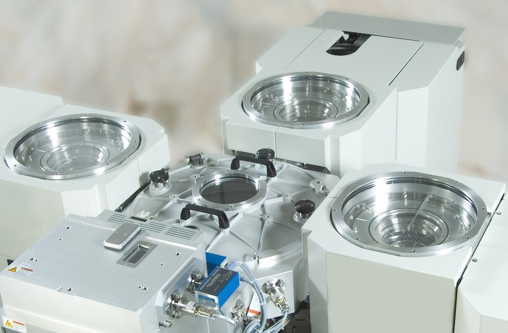
Xactix® c2L with 3 CVE modules
- Patented chamber design optimized for gas phase etching
- Edge lift to protect delicate double-sided wafers
- Temperature controlled chuck with optional backside helium for improved etch rates, uniformity and selectivity
- Easy conversion between 150 mm and 200 mm wafers
- Ability to clamp a wide variety of substrate thicknesses
- Wide range of wafer handling options
- Vapor release etch of MEMS
- microLEDs
- RF membranes
Xactix® X4
XeF2 Vapor Release Etch System
The Xactix® X4 xenon difluoride (XeF2) etch system features accelerated etch rates and superior components making it ideal for intensive R&D and pilot production. XeF2 shows high selectivity to silicon over almost all standard semiconductor materials including photoresist, silicon dioxide, silicon nitride and aluminum. The Xactix X4 system is easy to use, reliable and safe, it is the leading XeF2 etch system for releasing MEMS devices. Equipped with a patented dual expansion chamber design for high etch rates, the Xactix X4 system allows for high XeF2 gas flow and pressure without dilution from carrier gases. The system provides both pulsed and continuous flow etch processes. A unique expansion chamber-based design contributes to precise, repeatable pulse pressure and ease of mixing XeF2 with other gases. Customizable chamber size can be matched to the wafer size resulting in maximized etch rates, uniformity and efficiency.
- MEMS
- Photonics
- RF Device Manufacturing
Market Brochures
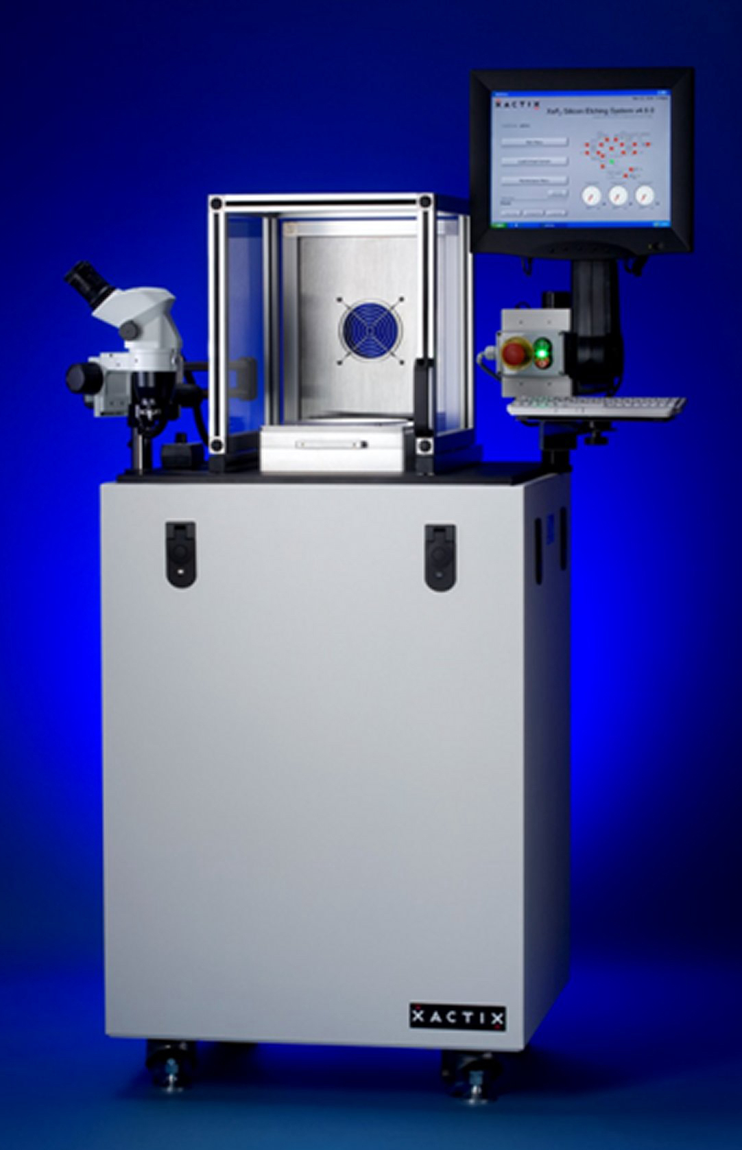
X4
- Equipped with a patented dual expansion chamber design for high etch rates
- Allows for high XeF2 gas flow and pressure without dilution from carrier gases
- Provides both pulsed and continuous flow etch processes
- Unique expansion-chamber-based design contributes to precise, repeatable pulse pressure and ease of mixing XeF2 with other gases
- Customizable chamber size can be matched to the wafer size resulting in maximized etch rates, uniformity and efficiency
- Easy to use, reliable and safe
- Vapor release etch of MEMS
- microLEDs
- RF membranes
Xactix® e2
Benchtop XeF2 Vapor Etch System for R&D
The Xactix® e2 xenon difluoride (XeF2) etch system is an ideal solution for those seeking a low cost, benchtop R&D etching system. Isotropic etching of silicon using XeF2 is an ideal solution for releasing MEMS or photonic devices. XeF2 shows high selectivity to silicon over almost all standard semiconductor materials including photoresist, silicon dioxide, silicon nitride and aluminum. Process flexibility is a key to successful research and the Xactix® e2 system provides the widest range of process options. The e2 offers ease of use, low cost of ownership, a small footprint and excellent process flexibility.
- MEMS
- Photonics
Market Brochures
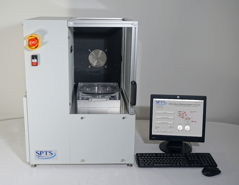
Xactix e2
- Low cost, easy to use, and reliable
- Great for working with small samples and wafers
- Includes the etch unit, PC with keyboard and mouse, flat panel display, pump, and manual
- Options to increase process flexibility
- Increased selectivity to SiN and SiO2
- Additional process gas can be added
- Pulsed and optional continuous flow etch processes
- Lower installation costs
- Easy field upgrades with options
R&D scale XeF2 etching
Are you sure?
You've selected to view this site translated by Google Translate.
KLA China has the same content with improved translations.
Would you like to visit KLA China instead?
您已选择查看由Google翻译翻译的此网站。
KLA中国的内容与英文网站相同并改进了翻译。
你想访问KLA中国吗?
If you are a current KLA Employee, please apply through the KLA Intranet on My Access.