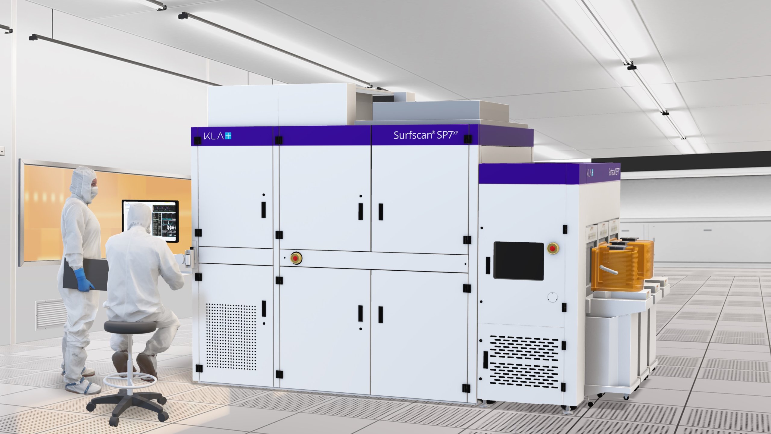
Today, KLA Corporation announced our new Surfscan® SP7XP wafer defect inspection system. This new member of our Surfscan family of inspectors discovers the smallest defects and imperfections on bare wafers and blanket films, helping semiconductor substrate, equipment, materials and chip manufacturers achieve the strict manufacturing quality standards needed to produce the most advanced chips. This ensures the functionality and reliability of the chips used in your electronic devices, so that you can continue to connect remotely, explore virtually and discover endlessly.
KLA’s multi-disciplinary team of engineers developed technologies that ensure our Surfscan SP7XP unpatterned wafer inspection system addresses a broad range of challenges associated with the integration of advanced semiconductor chips. Whether the industry challenge is finding the defects inhibiting development of the latest transistor technology or achieving the inspection sensitivity and speed needed for process monitoring in high volume manufacturing, the Surfscan SP7XP has the capability to address these challenges head on.
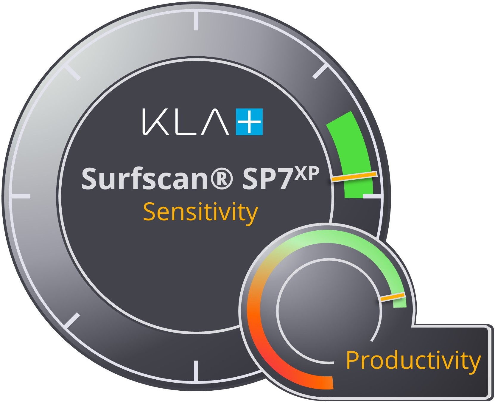
Ultimate Sensitivity The introduction of a 12.5nm inspection mode coupled with new low noise sensors provide the ultimate inspection sensitivity required for research and development pathfinding in advanced substrate, semiconductor equipment or chip manufacturing.
Productivity Higher throughput is now available for inspection modes used in high volume manufacturing (HVM) increasing semiconductor fab capacity for smaller design nodes and high-end film applications.
Normal Illumination (NI) Normal illumination is used to quickly detect unique defects like embedded deformities, scratches, sliplines, residue and defects with low material contrast.
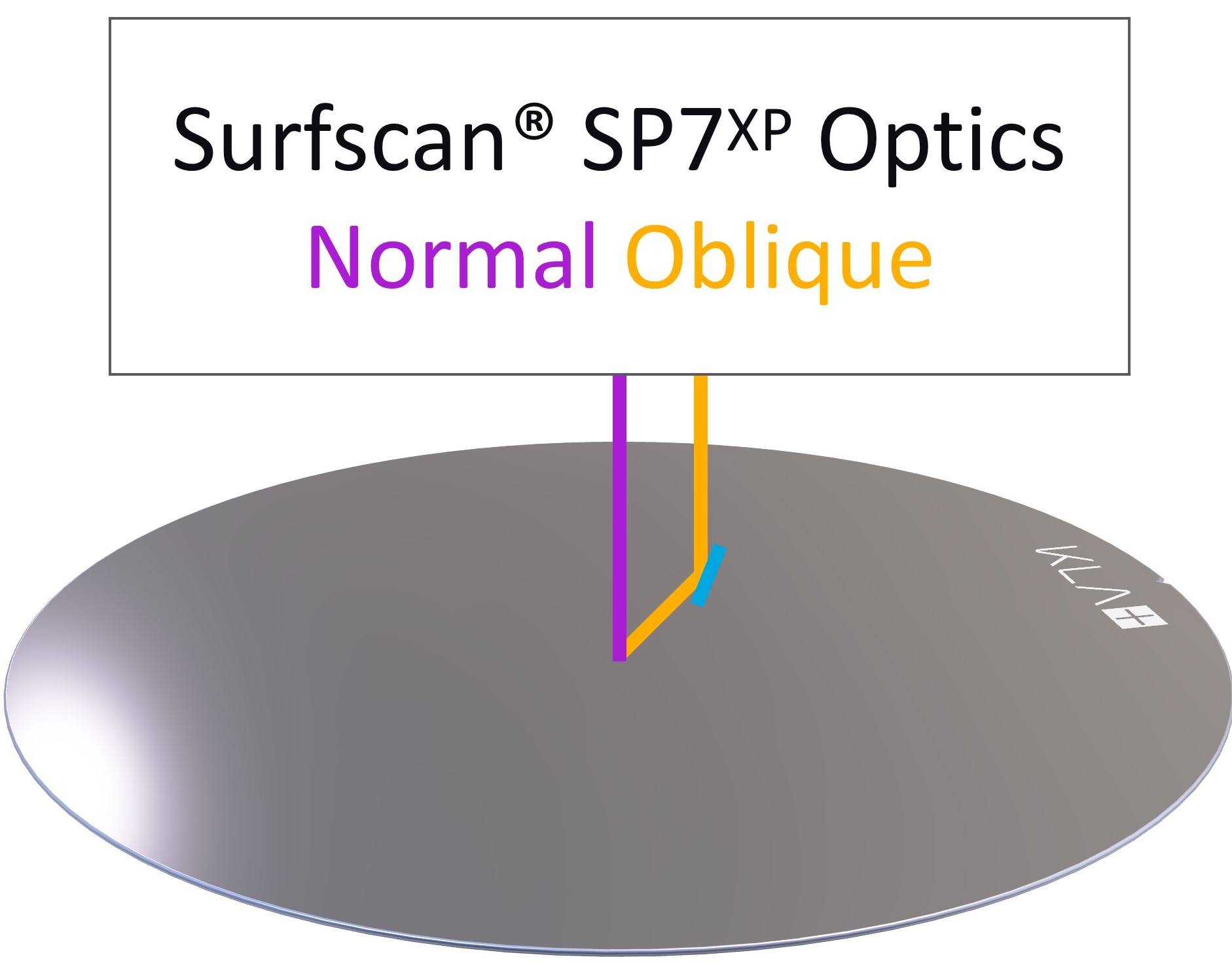
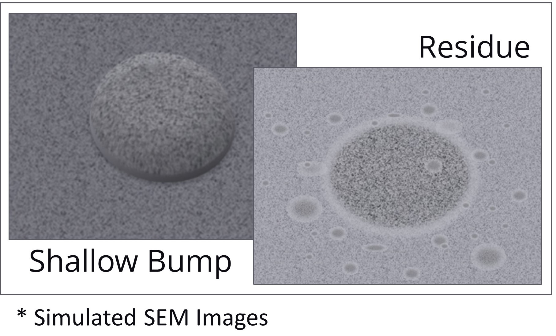
Phase Contrast Channel (PCC) Using normal or oblique illumination, the new phase contrast channel captures defect types with weak scattering such as shallow bumps and residue with increased sensitivity.
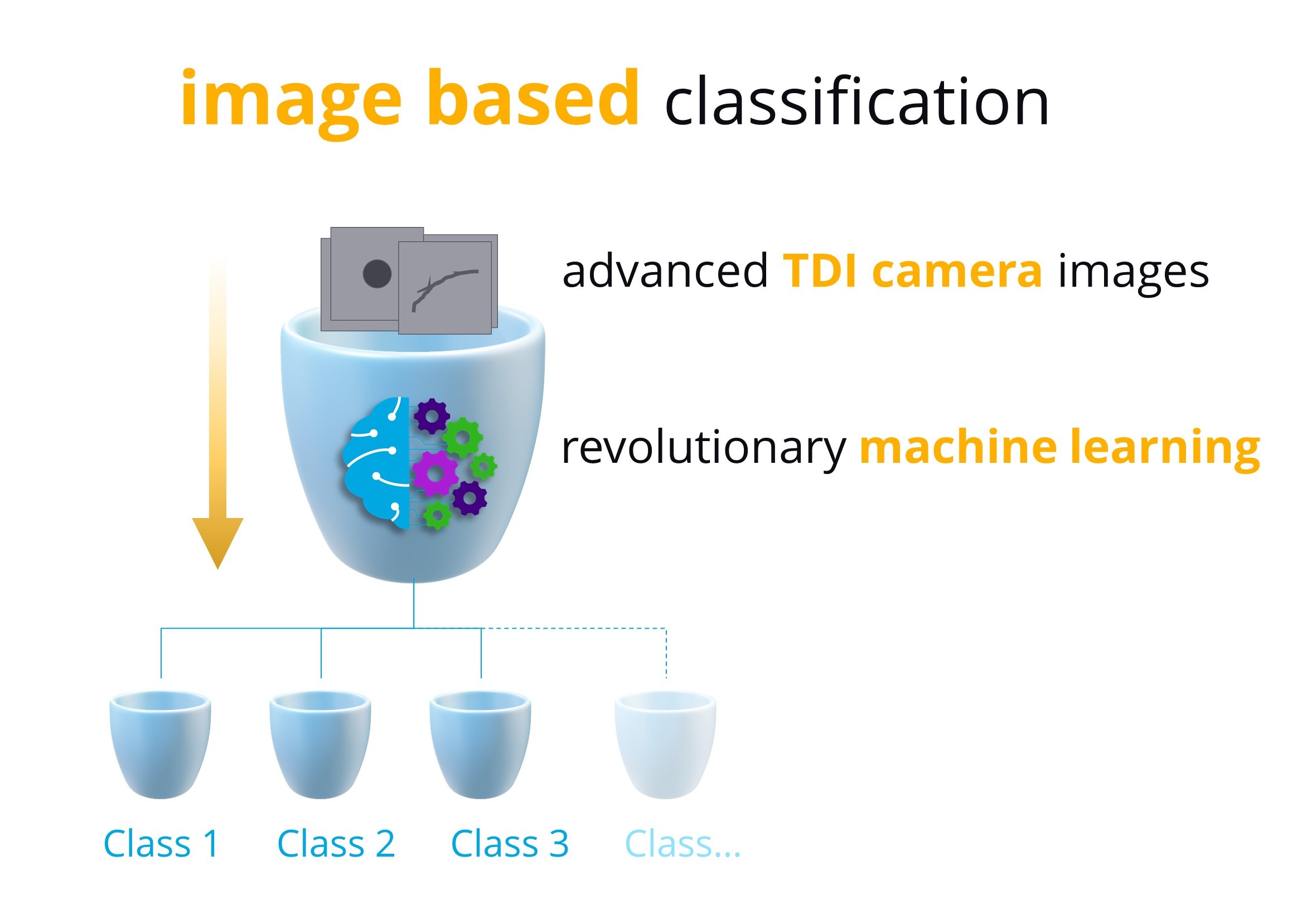
Image Based Classification: (IBC) The Surfscan SP7XP applies revolutionary machine learning algorithms to defect images to accurately classify defects, which in turn accelerates the time to root cause. IBC also facilitates faster setup of the classification recipe while improving classification accuracy and purity.
Z7™ Classification Engine Traditional destructive measurement techniques, where the substrate is cross-sectioned using a focused ion beam (FIB) and imaged with a scanning electron microscope (SEM), can be minimized with the introduction of the new Z7™ multi-channel defect classification algorithm. This innovative new classification engine enables classification of embedded defects for 3D NAND and other thick film monitoring applications facilitating the troubleshooting of excursions and building stronger correlation with inline monitoring.
SurfServer® The SurfServer recipe management system facilitates recipe portability and helps to streamline fleet management. The recipe distribution system (RDS) feature enables users to create recipes and synchronize them to all tools in their fab, resulting in faster recipe setup.
For more information on the Surfscan SP7XP unpatterned wafer inspection system, visit the product page, see our press release, or visit our virtual booth at SEMICON Japan!
Follow Us