As the world works to reduce greenhouse gas emissions, global adoption of electric vehicles (EVs) is driving an increased demand for high-power, energy-efficient compound semiconductors, such as silicon carbide (SiC)-based components, throughout the entire EV assembly process.
Renewable energy technology is now at the forefront of climate-forward research, with accelerating EV sales playing a bigger role than ever before. One key industry challenge: increasing overall electric vehicle efficiency.
KLA has been advancing humanity by delivering solutions and support to the SiC and gallium nitride (GaN) power device market that enables advances in EVs and other green technologies. Leveraging our vast experience in developing new technology capable of solving complex challenges across the IC industry to help drive yield improvements, we have developed a comprehensive portfolio of process equipment and inspection and metrology process control solutions specialized for the unique needs of power devices.
Our portfolio of products starts with inspection of SiC and GaN wafers, and we’ll share how KLA Instruments™ Candela® 8520 system is being used by manufacturers in the power electronics supply chain to improve substrate wafer quality and yield and optimize their epitaxial growth processes.
“The future of renewable energy is here, with a rapidly growing market and increased global adoption driving advances in green technology. KLA Instruments™ is supporting the SiC industry’s efforts to equip manufacturers of EV technologies with solutions to drive us toward a greener, healthier planet.”
James Costello, manager, New Product Introduction, KLA Instruments
Accelerating Electric Vehicle Adoption through Improved Power Efficiency

Increasingly, automotive OEMs and Tier 1 suppliers are switching from Si to SiC power semiconductor devices for their EV applications. Small, light, power-efficient SiC-based devices can handle high temperatures, making them well-suited to EV applications. Due to the impact of these technologies on vehicle performance, automakers are increasingly using higher-voltage, SiC-based systems to increase power efficiency for their EVs that enhance charge life and increase speed capability as well as towing capacity.
Innovating for SiC Device Manufacturers
SiC semiconductor device manufacturing has unique challenges compared to Si semiconductor manufacturing. Defects in the SiC substrate and epitaxial layer occur at a much higher density than in Si substrates, making it an important priority for manufacturers to detect the defects, as when left unchecked in a Si- or SiC-based power device, it can lead to system failure.
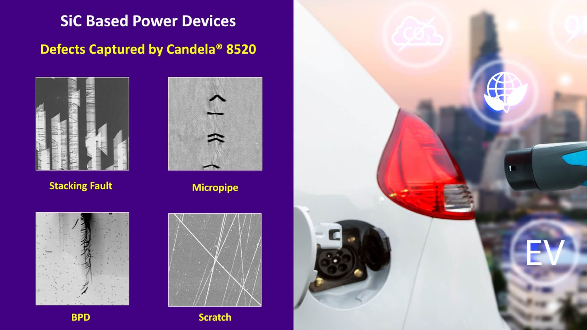
KLA Instruments’ Candela® 8520 system is designed specifically for identification of the SiC substrate and epitaxial defects. The 8520 system’s multi-detection channels help manufacturers uncover process-related issues and identify and classify yield-impacting defects including triangles, carrots, stacking faults, basal plane dislocations (BPDs), micropipes, scratches and more.

KLA Instruments’ Green Mission
The KLA Instruments group develops, markets and services metrology and defect inspection systems that are used by high-volume manufacturers (HVM) and research and development departments in universities and industrial labs. Our portfolio serves a broad range of markets including biotech and medical devices, optics, displays, batteries and energy technologies.
“The capability of our tools to benefit research and manufacturing in battery, solar and other green technologies continues to inspire us to innovate across a broad range of green technology applications,” said Tom Pierson, general manager, KLA.
Aligned with KLA’s ESG commitments and strategy, KLA Instruments supports manufacturers in renewable technologies striving to offer a greener future for our planet.
The Candela® 8520 joins the 8 Series and Surfscan® SP A2 in providing inspection capability for SiC and GaN power device manufacturing. To learn more about KLA’s full portfolio of products for power devices, check out our Compound Semi and Substrate Manufacturing web pages, and plasma etch processes for SiC and GaN-on-Si power devices from our SPTS division in this interesting article.
Follow Us