Product Description
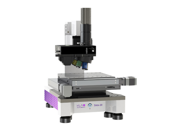
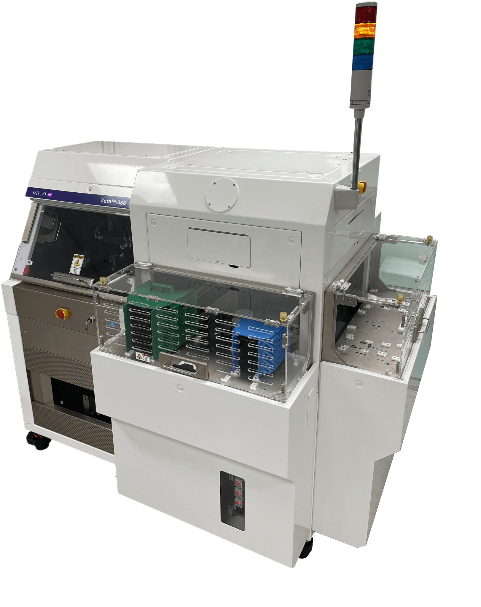
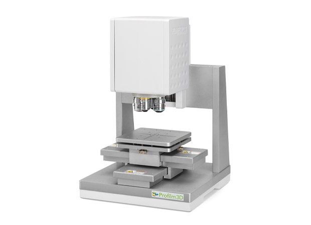
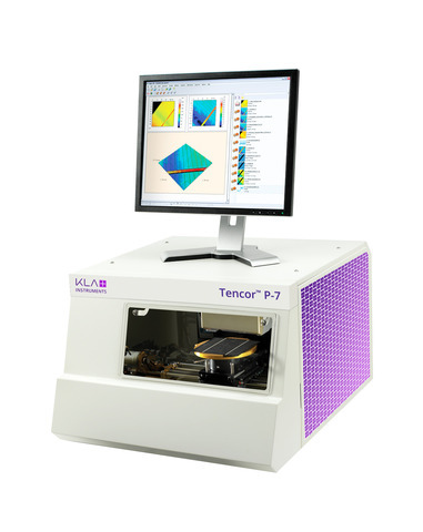
The Zeta-300 optical profiler is a non-contact, 3D surface topography measurement system. The Zeta-300 builds on the capability of the Zeta-20 3D profiler with additional isolation options and configuration flexibility to handle larger samples. The 3D optical metrology system is powered by patented ZDot technology and Multi-Mode optics, enabling measurement of a variety of samples: transparent and opaque, low to high reflectance, smooth to rough texture, and step heights from nanometers to millimeters.
The Zeta-300 optical profiler non-contact measurement system integrates six different optical metrology technologies in one configurable and easy-to-use system. ZDot measurement mode simultaneously collects a high-resolution 3D optical scan and a True Color infinite focus image. Other 3D optical metrology techniques include white light interferometry, Nomarski interference contrast microscopy, and shearing interferometry. Film thickness can be measured with ZDot or an integrated broadband reflectometer. The Zeta-300 is also a high-end microscope that can be used for sample review or automated defect inspection. The Zeta-300 3D profiler supports both R&D and production environments by providing comprehensive step height, roughness, and film thickness measurements and defect inspection capability.
Features
- Easy to use optical profiler with ZDot and Multi-Mode optics to address a wide range of applications
- High-quality microscope sample review or defect inspection
- ZDot: Simultaneously collects a high-resolution 3D scan and a True Color infinite focus image
- ZXI: White light interferometry for wide area measurements with high z resolution
- ZIC: Interference contrast for quantitative 3D data of surfaces with sub-nanometer roughness
- ZSI: Shearing interferometry for images with high z resolution
- ZFT: Film thickness and reflectance is measured with an integrated broadband reflectometer
- AOI: Automatic optical inspection to quantify defects on the sample
- Production capability: Fully automated measurements with sequencing and pattern recognition
Applications
- Step height: 3D step height from nanometers to millimeters
- Texture: 3D roughness and waviness on smooth to very rough surfaces
- Form: 3D bow and shape
- Stress: 2D thin film stress
- Film thickness: transparent film thickness from 30nm to 100µm
- Defect inspection: capture defects greater than 1µm
- Defect review: KLARF files are used to navigate to defects to measure 3D surface topography or scribe defect locations
Industries
- LED: light emitting diodes and PSS (patterned sapphire substrates)
- Semiconductor and compound semiconductor
- Semiconductor WLCSP (wafer-level chip scale packaging)
- Semiconductor FOWLP (fan-out wafer-level packaging)
- PCB (printed circuit board) and flexible PCB
- MEMS: Micro-electro-mechanical systems
- Medical devices and microfluidic devices
- Data storage
- Universities, research labs and institutes
- And more: Contact us with your requirements
