KLA Innovation: Broadband Plasma Optical Inspection for Chip Manufacturing
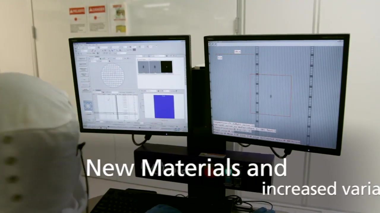
May 14, 2021KLA’s broadband plasma optical patterned wafer defect inspection systems enable discovery of yield-critical defects on advanced memory and logic devices. With broadband plasma illumination, advanced optics and innovative design-aware technologies, these inspectors capture critical defects across a range of process layers at optical inspection sped, providing Discovery at the Speed of Light™.